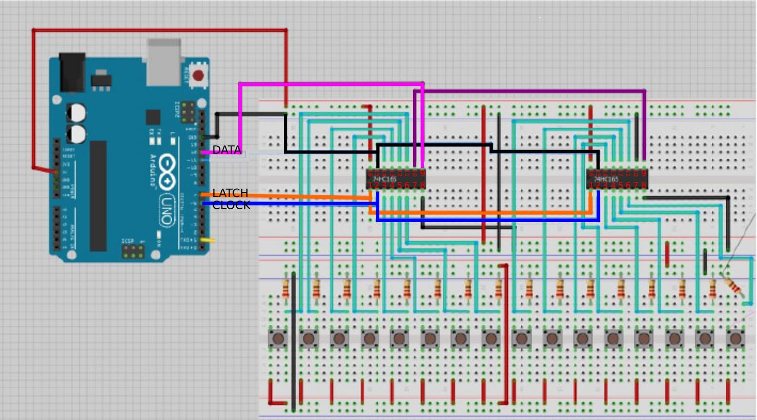
What where should I connect these 74HC165 pins to my KSOLOTI board?
CLK INH, QH, CLK, SH LD
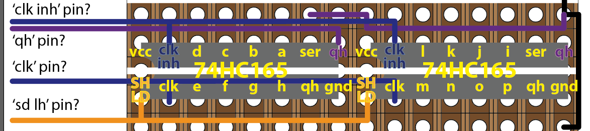
Edit: fixed pinout
Hi,
-
I suggest you get yourself familiar with chaining 74HC165 shift registers (generally called PISO shift registers) - some short Arduino tutorial should be enough. Shift registers are blatantly straightforward but really hard to wrap your head around! I find myself trying to count the clock cycles and trying to figure out how the signal shifts when certain pins are low or high - gives me headaches. Here is a schematic that might help you figure out the connections.
-
“CLK INH” (also called ~CE) should be tied to Ground as the Axoloti/Ksoloti object does not use it.
-
The following pins can (must) be connected to any GPIO on Ksoloti - Select which GPIO you want to connect:
- “data”:
SER (also called DS or SDATA)QH (also called Q7), - “clock”: CLK (also called CP),
- “latch”: SD/LH (also called ~PL)
- “data”:
-
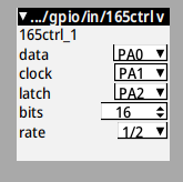
I’ve added updated 165ctrl v and 165in objects at kso/gpio/in/ (File > Sync Libraries to pull the latest changes).
-
Also check out the help patch by right-clicking on the object title at the top.
-
Select how many “bits” you want to read. Since in your screenshot you seem to be using two HC165, so reading up to 16 bits is possible. Their states will be available as bits 0…15 in the 165in objects. Note that the effective bit order may be reversed in respect to the pin names D0..D7 (also called A..H) on the HC165. Bit0->D7, bit1->D6, and so on. Long story, mostly has to do with efficiency and bit order of the shift register stream (MSB first).
-
Edit: QH of the second HC165 should connect to SER (also called DS or SDATA) of the first HC165. This will forward the serial data coming in from the second HC165 so we can read both (or more) HC165’s through the first one’s QH pin. If you chain more than two HC165’s, QH of the third HC165 goes to SER of the second HC165, and so on. Check with online schematics to figure out where data and QH go. The schematic linked above is tested and works for me.
1 Like
You’re not wrong ![]() SER/DS/SDATA is the input pin, QH/Q7 is the overflow output pin. When you’re sending out the bitstream the first chip fills up and once it’s got its data it overflows through QH into the next one, and once that’s filled it would overflow further and further down the line.
SER/DS/SDATA is the input pin, QH/Q7 is the overflow output pin. When you’re sending out the bitstream the first chip fills up and once it’s got its data it overflows through QH into the next one, and once that’s filled it would overflow further and further down the line.
I’m wrong. Ignore this post and look further down ![]()
1 Like
Nice, perhaps I got confused and read the ucapps.de schematic in the wrong direction. So would J2 be the header that connects to Ksoloti, and J1 the header for chaining additional 165’s?
You’ve got me doubting myself now, so I’ve gone back to my datasheet collection and I’m still doubting myself. It’s how a 595 is wired, it may be that I was thinking of that? I’ll try and work it out, and if I’m wrong I’ll report back.
Ignore everything I just said, I was thinking about 595s and outputs.
I tested it over on Wowki, the documentation for it is here:
QH/Q7 is still where the data flows out of, but of course we want to be reading that data, not writing it. So that’s what gets connected to the GPIO, and you were right to be unsure.
I’m very sorry! In my defence I’m not feeling well ![]() and trying to distract myself…
and trying to distract myself…
Nice, well it was my mistake to begin with!
I am more familiar with 595 as well.
I have edited my response above.
What got me (us?) confused is the data pin labeled SER/SDATA - seems natural to use it as, well, the data pin. But checking with the datasheet, this is not an output! We obviously need an output pin to go high and low so we can read the bit states… enter QH.
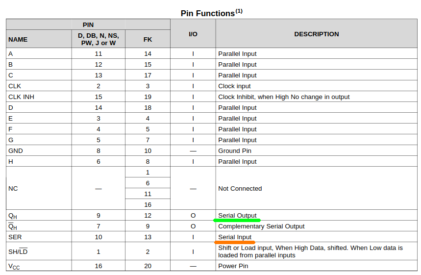
Bit of a mislabeling if you ask me, they could have called it SI or FWD or whatever but oh well.
Anyway, no need to feel sorry but the opposite. Our discussion lead to the right results after all. Hope you’re feeling better soon!
2 Likes